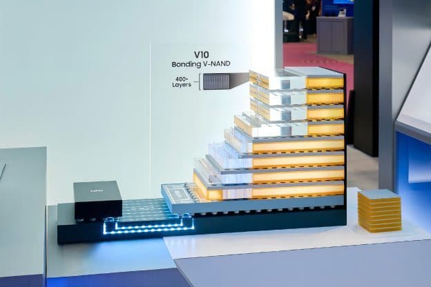
Samsung used FMS 2026 in Santa Clara on 5 August to show what it wants AI memory to look like in three dimensions. Three things were announced, and only one of them is a product.
The shipping part
V10 BV-NAND passes 400 layers, an industry first, built with wafer bonding and a 3-stack structure. Density rises 58% over the V9 generation, with better read/write and I/O speed. Samsung says it is in mass production and supplied to Nvidia. SK hynix's competing 375-layer enterprise SSD is due to enter production in early 2027.
The concepts
zHBM moves HBM from beside the accelerator to directly above it, and allows custom IP between memory and logic for application-specific designs. The headline claim — up to eight times the performance of HBM5 — attaches to a concept model, not silicon anyone can buy. zNAND-O aims at on-device AI in PCs, phones, robots and servers, combining DRAM-like speed with NAND-like capacity. Neither has a production date.
Why stack at all
Side-by-side HBM burns power and latency on the interposer traces between logic and memory. Stacking shortens the path. It also concentrates heat in the worst possible place — directly over the hottest die — which is the engineering reason nobody ships this yet.
Reading the announcement correctly
HBM5 itself is not in volume production. A number expressed as a multiple of an unshipped generation, from a concept model, is a roadmap position. The 400-layer NAND is the news; the 8x is the pitch.