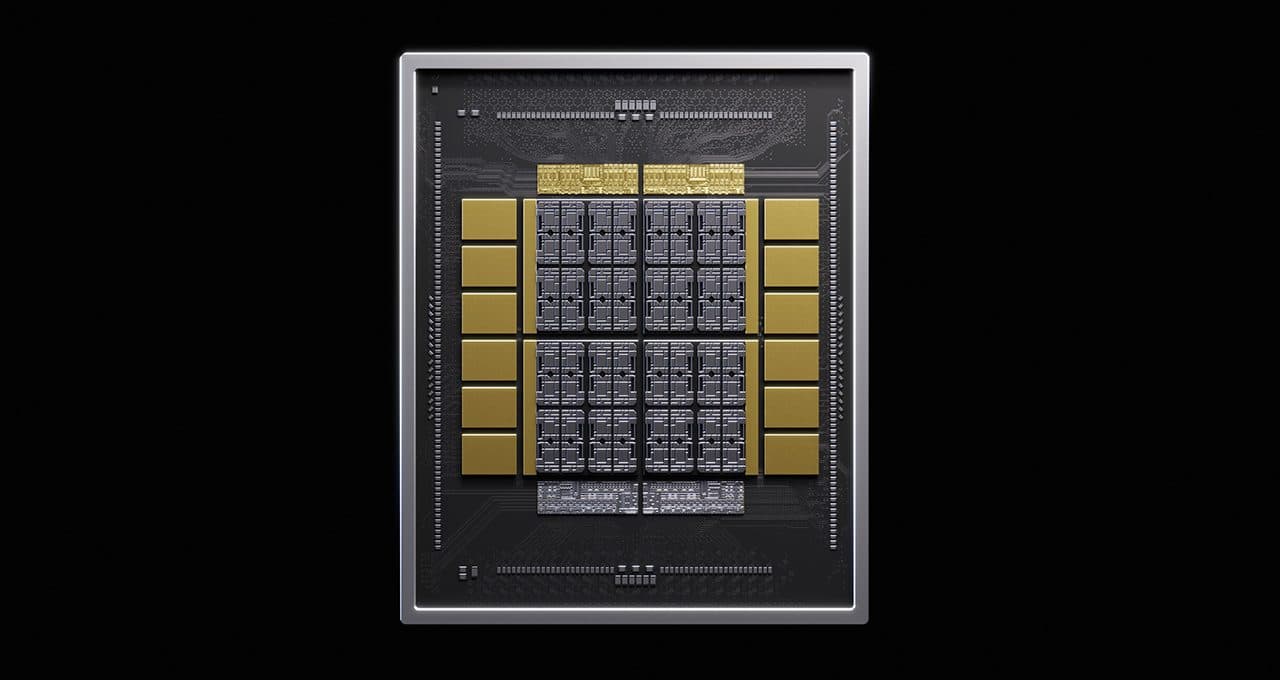
Nvidia published a blog post on 26 August at 21:05 UTC introducing NVHBM, described alongside NVLink Fusion as custom high-bandwidth memory. Read quickly, it says Nvidia is now in the memory business. Read closely, it says something narrower and more interesting.
What NVHBM actually is
In a conventional stack, the memory controller sits on the processor die and talks to HBM across a physical interface. Nvidia's proposal moves that controller into the base die of the HBM stack itself. The company describes it as "establishing a standard NVHBM implementation, available from multiple memory providers." Nvidia designs the controller and the interface; somebody else fabricates and stacks the DRAM. This is a licensing and specification play, not a manufacturing one.
The three numbers, and their denominator
The post makes three quantitative claims: up to 30% greater memory bandwidth, 15% lower HBM power consumption, and freeing up to 25% more area on the XPU compute die. All three are stated against standard HBM4E. That matters twice over. First, each is an "up to" figure, which is a ceiling rather than an expectation. Second, HBM4E is itself a forward-looking part — the comparison is between one unshipped specification and another, not against memory anyone can buy today.
What the common framing gets wrong
The natural summary — "Nvidia is building its own HBM" — inverts the arrangement. Nvidia is doing the opposite of vertical integration here: it is standardising an interface so that several suppliers can build to it, which increases its leverage over memory vendors precisely because it does not depend on one. The second misreading is the area figure. "Frees up to 25% more area on the compute die" is being repeated in places as a compute gain of around 30%, which the post does not claim. Freed silicon area is an opportunity to add compute in a future design, not a speed-up in an existing one. Nothing on the market gets faster because of this announcement.
What is missing
There is no named memory supplier. Given that the entire concept depends on "multiple memory providers" agreeing to build base dies to Nvidia's specification, the absence of a single named partner from Samsung, SK hynix or Micron is the most substantive gap in the announcement. There is no ship date and no product it appears in. The one named party is Amazon's Annapurna Labs, described as the first to work on NVHBM alongside NVLink Fusion — collaboration on the technology, not a committed deployment.
Why Nvidia wants the controller moved
Memory bandwidth, not arithmetic, is the constraint on large-model inference, and the physical interface between processor and memory consumes a growing share of both die area and power budget. Owning the controller specification lets Nvidia tune that interface to its own architectures while keeping several fabs competing to supply the parts. If the specification is adopted, the strategic gain is durable. If it is not, nothing was manufactured and nothing was lost.